ブックタイトル豊田工業大学 2018
- ページ
- 56/68
このページは 豊田工業大学 2018 の電子ブックに掲載されている56ページの概要です。
秒後に電子ブックの対象ページへ移動します。
「ブックを開く」ボタンをクリックすると今すぐブックを開きます。
このページは 豊田工業大学 2018 の電子ブックに掲載されている56ページの概要です。
秒後に電子ブックの対象ページへ移動します。
「ブックを開く」ボタンをクリックすると今すぐブックを開きます。


豊田工業大学 2018
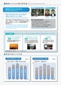
機械システム分野の研究室Mechanical Systems Engineering Laboratories 電子情報分野の研究室Electronics and Information Engineering Laboratories研究の受け入れ状況Me c h a n i c a l Sy st ems En g i n e e r i n g L a b o r a t o r i e s助教 南部 紘一郎Assistant ProfessorKoichiro Nambu教授 奥宮 正洋ProfessorMasahiro Okumiya組織・表界面制御に基づき材料機能を極限まで高めるプロセス開発Development of novel materials processing for the upmost improvement inmaterial functions through the microstructure, surface and interface control構造材料の物理的、化学的、機械的性質を極限まで高めるプロセス開発が研究テーマ、独創的なアイデアに基づくミクロ組織、表面構造制御あるいは異相界面制御を骨子とするプロセスにより、材料機能の飛躍的向上や創成を目指している。The research programs are focused on the development of novel processingfor the upmost improvement in physical, chemical and mechanical propertiesof structural materials. They are aimed at achieving the upmost improvementin material functions through the microstructure, surface and interface controlbased on the original innovative ideas.主な研究テーマMain Research ThemesSurface modification of aluminum using barrel-nitriding and ion-nitriding■バレル窒化とプラズマ窒化によるアルミニウムの表面改質Utilizatiom of natural gas in gas carburizing.■天然ガスを有効利用したガス浸炭プロセスの開発Structural control of cast aluminum alloys through ultrasonic sono-solidification■超音波ソノ凝固によるアルミニウム合金鋳造材料の組織制御Prevent of unusual brittle fracture in bearings by the additional micro particle on grease.■グリースへの微粉末添加による軸受けの白色剥離防止URL:http://ttiweb.toyota-ti.ac.jp/1432/pub_semi_show.php?n=14材料プロセス研究室Materials Processing LaboratoryMagnetron sputteringマグネトロンスパッタリング装置研究設備・研究のイメージResearch Equipment and Subjects 教員Faculty MemberEl e c t r o n i c s a n d I n f o rma t i o n En g i n e e r i n g L a b o r a t o r i e s次世代のクリーンなエネルギーを担う、高効率太陽電池および材料の研究Research and development of high efficiency solar cells and materialsfor the new clean energy source in the next generation太陽光発電は21世紀を担うクリーンな新エネルギー源の中核に位置付けられる。極限効率を目指した超高効率多接合構造太陽電池、結晶シリコン太陽電池、集光型太陽電池や太陽電池用新素材など、各種半導体材料・デバイスついての研究を行っている。Photovoltaic(PV)power generation is the key technology for the new energysource of the 21st century. We study various semiconductor materials anddevices, including super-high efficiency multi-junction solar cells to achieveultimate conversion efficiency, crystalline Si solar cells, concentrator solarcells and other innovative new solar cell materials.ProfessorYoshio Ohshita教授 大下 祥雄助教 小島 信晃Assistant ProfessorNobuaki KojimaSemiconductor crystal growthby molecular beam epitaxy分子線エピタキシー装置による半導体結晶成長主な研究テーマMain Research ThemesURL:http://ttiweb.toyota-ti.ac.jp/1432/pub_semi_show.php?n=17Study on concentrator solar cellsStudy on high-efficiency solar cells■高効率太陽電池の研究Study on new solar cell materials and principles■太陽電池用新素材・新原理の研究■集光型太陽電池の研究Study on novel opto-electronic functional materials■機能性光・電子材料の研究rm半導体研究室Semiconductor Laboratory研究設備・研究のイメージResearch Equipment and Subjects 教員Faculty Memberss主な研究テーマMain Research Themes教授 岩田 直高ProfessorNaotaka Iwata研究設備・研究のイメージResearch Equipment and Subjects省エネルギー社会に向けて、高効率動作する低コスト高機能半導体デバイスを開発Development of low-cost high-functionality semiconductor deviceswith high efficiency operation for the energy conservation society生活に不可欠な電子機器を構成する低コスト半導体デバイスの省電力化と高機能化に大きな注目が集まっている。これに対処するため、本研究室は、半導体材料、製造プロセス、デバイスおよび応用に関する技術の研究を行っている。Much attention has been paid on cost reductions, power savingoperations and high functionalities of semiconductor devices constitutingelectronic products indispensable to our lives. To address it, the AdvancedElectron Devices Laboratory investigates semiconductor materials,Advanced Electron Devices Laboratory電子デバイス研究室Compound semiconductor heterojunctionFET fabricated作製した化合物半導体ヘテロ接合FETAtomic layer depositionapparatus原子層堆積装置Compound semiconductor heterojunction devices on Si substrates■Si基板上の化合物半導体ヘテロ接合デバイスの研究Compound semiconductor sensors with novel features■新機能化合物半導体センサの研究Ultra-low energy consumption semiconductor devices and systems■超低消費電力半導体デバイスとシステムの研究URL:http://ttiweb.toyota-ti.ac.jp/1432/pub_semi_show.php?n=49教員Faculty Member(件数)(年度)受託研究・共同研究の受け入れ実績(過去5年間)0共同研究受託研究102030405060708090735617外部からの研究費受け入れ実績(過去5年間)(百万円)1000200300400500600700800900(年度)企業等民間から文部科学省等公的機関から84620122013201420152016849180726546226972746684206890638627222 20820122013201420152016856520807120512159932073fabrication processes, devices and application technologies.フォトニックデバイスや光波の物理を熟考し斬新な光システム機能を創成Photonic systems with novel functions are created, considering deeplyphysical phenomena in photonic devices and lightwaves.光デバイスや光波の物理を熟考し斬新な機能を有する光システムを構築する。光ファイバの伸縮歪を数mm分解能で分布計測する光システムや光波の干渉特性を合成する独自技術による光情報処理システムなどの研究を行う。本分野をシステムフォトニクスと呼ぶ。Photonic systems with novel functions are created, considering deeply physicalphenomena in photonic devices and lightwaves. Examples are photonic systemsfor measuring distributed strain along an optical fiber with mm order spatial resolutionand those for signal processing by original schemes to synthesize arbitrarily opticalinterference properties. This research area is called "Systems Photonics."主な研究テーマMain Research ThemesFiber optic nerve systems for structures that can feel pain■痛みの分かる構造の為の光ファイバ神経網技術の研究Distributed optical fiber strain and/or temperature sensing with Brillouinscattering in an optical fiber as a sensing mechanism■光ファイバ中のブリルアン散乱を計測原理とした分布型歪・温度センシング技術の研究Photonic information processing with synthesis of optical coherence function■光波コヒーレンス関数の合成による光情報処理技術の研究ProfessorKazuo Hotate教授 保立 和夫システム光波工学研究室Systems Photonics Laboratory研究設備・研究のイメージResearch Equipment and Subjects 教員Faculty MemberExperimental setup of an photonic system for measuring straindistribution along an optical fiber.光ファイバに沿う歪分布を計測するフォトニックシステムの実験系開かれた大学として地域社会・産業界に貢献できる取り組みを行っています。半導体プロセス実習・講習会半導体技術全般の知識を習得するための技術実習・講習会を開催しています。有料企業・学校関係者対象企業向けオープンラボ産学接点のための研究室見学会を開催しています。保有する実験設備・装置などを見学しながら研究の活動状況を知ることができます。無料企業・研究機関・大学関係者対象公開講座本学の研究活動を広くご紹介するため、科学技術に関する講演会を開催しています。無料一般対象※開催時期・募集方法などの詳細に関しては、ホームページにてご案内いたします。イベントの紹介URL:http://ttiweb.toyota-ti.ac.jp/1432/pub_semi_show.php?n=543 4