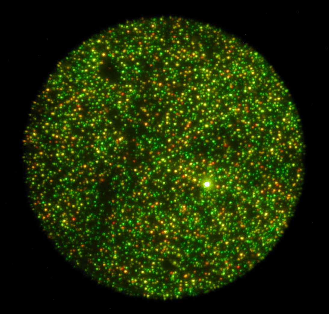
Micro PL
image of colloidal CdSe QDs spun coat on glass slide.
The color of the QDs
represent the degree of quantum confinement
(Collaboration with Mitsubishi
Chemical Corp. and RIKEN)

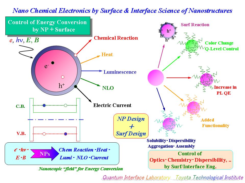
We prepare nano- and quantum structures, mainly semiconductors, and study the opto-
and electronic properties of their surfaces and interfaces to develop optical, eletronic,
and/or chemical devices such as catalysts..
Optoelectronic devices and catalysts, could ordinarlily be taken to be something totally
different. However, when we focus on the control of surfaces/interfaces of nano-/quantum
structures, the same material can be tuned to function as either or both. We wish to
turn this dream into reality through intensive investigation on the electronic properties
of surfaces and interfaces.
The diagram above explains the concept of "nano-chemical electronics" which IK has
been proposing for the last decade or so.
The fun and advantages of dealing with nano- and quantum structures are
1) integration of devices through minituarization,
2) the use of quantum effects, and
3) enhancement of surface/interface effects through increased surface
to volume ratio.
We are particularly interested in 2) and 3).
If the quantum structure is made of a semiconductor, quantized electronic states
in both valence band and conduction band are formed. By exciting the structure
from the outer world, the electron in the valence band quantized state can be
excited to the conduction band state. When this state relaxes, the excess energy
needs to be dissipated in some way. If this is done by throwing out a photon,
this is called luminescence or fluorescence. However, there are other possibilities
such as emission of heat or non-linear optical response. Furthermore, there are
cases when the energy is not relaxed but rather accumulated in the structure through
capture of carriers at surfaces or interfaces. If such carriers contribute to chemical
reactions of the outer world, this material is known to be catalyst.
Such "functions" are primarily determined by the selection of the material, and
then by the size of the quantum structures. However, we would like to emphasize
that the final fine tuning is done through surface/interface structures, and quite
drastically.
ところで、化学の世界では微粒子(ナノとは限らない)の表面に界面活性剤を付着させて
粒子の機能化を図る事は長年行われてきています。 特に、溶媒への分散に関するノウハウ
の蓄積は目を見張るものがあります。 これに加えて近年は、抗体抗原反応の様な生物的な
機能を持った分子の付着等も実現してきています。 しかし、表面への分子吸着はこれに
留まらず、上述の様に微粒子の電子物性自体の制御のためにも利用され始めております。
当研究室では、こうした、表面・界面の制御と機能化により、新規の物性や応用を探ります。
Past Events 2015
|
Date |
Title | Details |
|---|---|---|
|
Mar. 17, 2015 |
MBE maintenance | Repair of cell shutters, replacement of e-gun, etc. |
| Mar. 22, 2015 | Farewell Party | @Nagoya |
| Apr. 1, 2015 | Welcome Party | 山崎川花見+コンパ |