


Electronics and Information Engineering Laboratories
Memory Engineering Laboratory
Basic Information
Staff |
|
|---|---|
Outline |
Creating new functional materials via spin control of nanostructures Nanometer-sized spin materials, which enable electron spin control, are expected to lead to new functional devices. Our laboratory is committed to innovating spin metamaterials to develop ultra-low power petabyte memories(magnetic and/or optical) and to addressing global warming and other energy-related problems. |
Research Themes |
Petabyte stacked spin memories(SSMs), |
Equipment
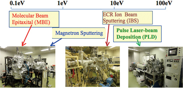
1 Sample preparation equipments
UHV chamber with MBE (Molecular Beam Epitaxy) and Magnetron Sputtering
UHV Ion Beam Sputtering and dry etcher
PLD (Pulse Laser Deposition)
2 Nano Size Processing
EB (Electron Beam) Lithigraphy
FIB (Focused Ion Beam Processing
3 Heat Processing
Nano-imprint
Induced heating anneal
Lamp heating anneal
4 Sample shape evaluation equipments
SEM (Scanning Electron Microscope )
AFM (Atomic Force Microscope )
MFM (Magnetic Force Microscope )
Polarized-Optical Microscope with external field and focused Laser
Optical Microscope (x100)
Surfcorder
5 Sample Characteristic Measurement equipments
EDX (Energy Dispersive X-ray Fluorescence Spectrophotometer)
VSM (Vibrating Sample Magnetometer) with superconducting magnet
Hall Effect Measurement System
VSM (Vibrating Sample Magnetometer) with electromagnet
AGFM (Alternating Gradient Force Magnetometer )
Polar Kerr Curve Tracer (Perpendicular to the film)
Magneto-Optical Kerr and Ellipticity Measurement System
Ellipsometer
Activities
![]()