Low-cost high-functionality semiconductor devices with high efficiency operation for the energy conservation society
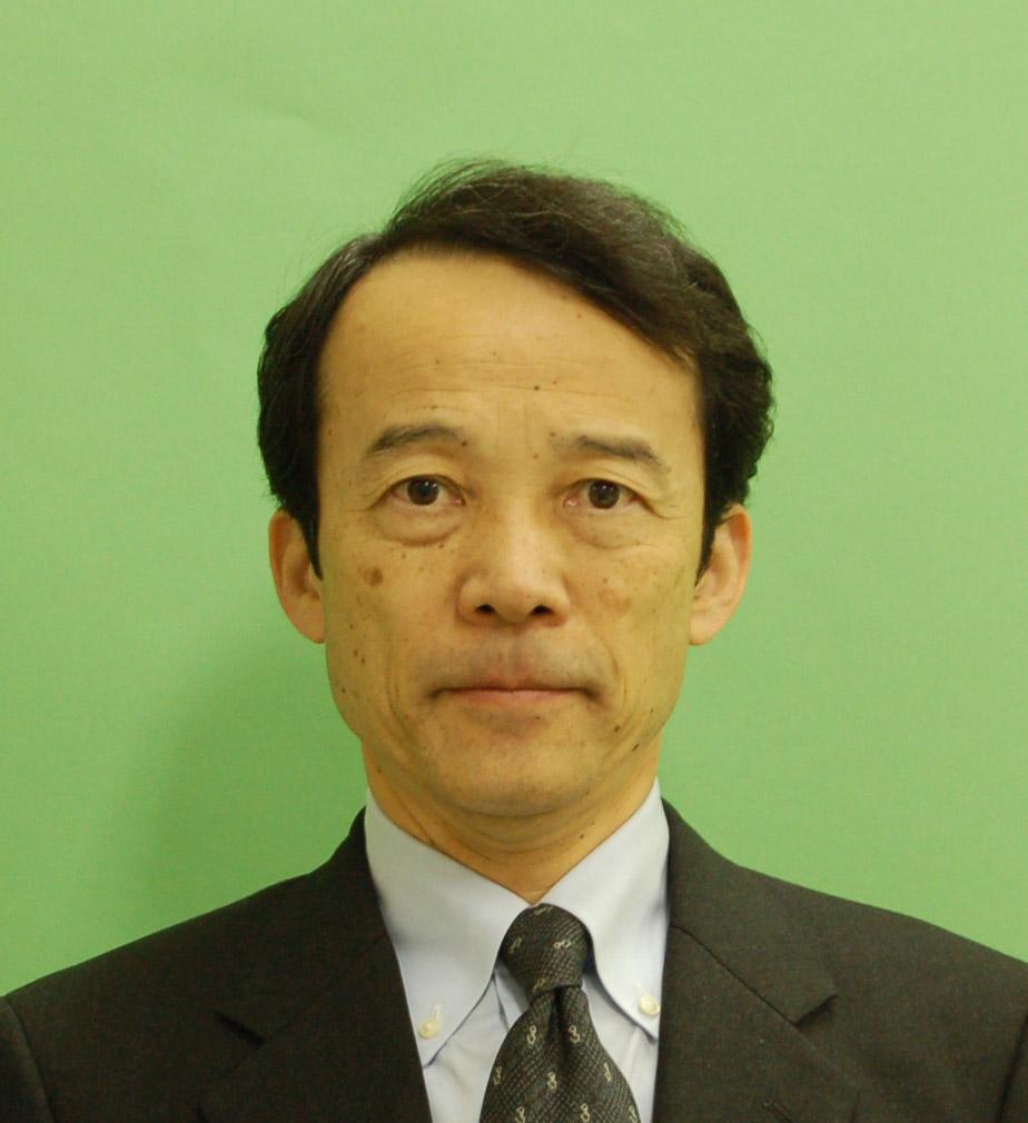
[Professor] Naotaka Iwata
Basic Information

Naotaka Iwata
Degree |
Doctor (Engineering) |
|---|---|
Laboratory Name |
|
Research Fields |
Low-cost high-functionality semiconductor devices with high efficiency operation for the energy conservation society |
Keywords |
compound semiconductor, semiconductor devices, fabrication process, low energy consumption |
E-mail Address |
|
Academic Background |
Doctor (Engineering), Universiy of Tsukuba (1999/3/25) |
Work History |
Professor, Toyota Technological Institute (2013/4-Present) |
Membership of Academic Societies |
Senior Member, IEEE (the Institute of Electrical and Electronics Engineers) |
Research Themes
Compound semiconductor heterojunction power devicesCompound semiconductor sensors with new functionality
Ultra-low energy consumption semiconductor devices and systems
Original Papers
[Academic Year] 2022[Articles] Breakdown voltage enhancement of p-GaN/AlGaN/GaN diode by controlling Mg acceptors for compensating residual Si donors
[Author] S. Kawata, Y. Zhang, and N. Iwata
[Date of Issue] 2022/11
[journal] Jpn. J. of Appl. Phys. Vol. 62, SA1004-1-5
[Academic Year] 2021
[Articles] High breakdown voltage of AlGaAs/GaAs/AlGaAs diode achieved by balanced charges considering residual carbon impurity in hole and electron channels
[Author] H. Ogawa, S. Kawata, and N. Iwata
[Date of Issue] 2021/4
[journal] Jpn. J. of Appl. Phys. Vol. 60, pp.041001-1-5
[Academic Year] 2020
[Articles] Effect of C- and Fe-doped GaN buffer on AlGaN/GaN HEMT performance on GaN substrate using side-gate modulation
[Author] M. E. Villamin, T. Kondo, and N. Iwata
[Date of Issue] 2021/3
[journal] Jpn. J. of Appl. Phys. Vol. 60, pp. SBBD17-1-8
[Academic Year] 2020
[Articles] High-selectivity dry etching for p-type GaN gate formation of normally-off operation high-electron-mobility transistor
[Author] N. Iwata and T. Kondo
[Date of Issue] 2020/10
[journal] Jpn. J. of Appl. Phys. Vol.60, pp. SAAD01-1-5
[Academic Year] 2019
[Articles] Effects of p-GaN gate structures and fabrication process on performances of normally-off AlGaN/GaN high electron mobility transistors
[Author] T. Kondo, Y. Akazawa, and N. Iwata
[Date of Issue] 2019/11
[journal] Jpn. J. Appl. Phys. Vol.59, pp. SAAD02-1-4
[Academic Year] 2017
[Articles] Laser-induced local activation of Mg-doped GaN with a high lateral resolution for high power vertical devices
[Author] N. Kurose, K. Matsumoto, F. Yamada, T. M. Roffi, I. Kamiya, N. Iwata, and Y. Aoyagi
[Date of Issue] 2018/1
[journal] AIP Advances Vol.8, pp.15329-1-5
[Academic Year] 2014
[Articles] Formation of conductive spontaneous via holes in AlN buffer layer on n+Si substrate by filling the vias with n-AlGaN by metal organic chemical vapor deposition and application to vertical deep ultraviolet photo-sensor
[Author] N. Kurose, N. Iwata, I. Kamiya, and Y. Aoyagi
[Date of Issue] 2014/12
[journal] AIP Advances Vol.4, pp.123007-1-7
Reviews
[Academic Year]2009[Articles]GaAs Switch ICs for Cellular Phone Antenna Impedance Matching
[Author]N.Iwata, and M.Fujita
[Date of Issue]2009/3/19
Books
[Academic Year]2002[Books]Microwave Technology Lecture Vol.6, "Integrated Circuit and Application," Chapter 3
[Author/Editor]N. Iwata
[Date of Issue]2002/6/25
Conference Presentations
[Academic Year] 2022[Title] Drain current lag characterization of Fe- and C-doped GaN buffer HEMTs on GaN substrates
[Academic Society] the 15th International Symposium on Advanced Plasma Science and its Applications for Nitrides and Nanomaterials (ISPlasma2023)
[Speakers] M. E. C. Villamin and N. Iwata
[Date of Presentation] 2023/3/7
[Academic Year] 2021
[Title] High breakdown voltage of p-GaN/AlGaN/GaN diode with controlled Mg acceptor charges
[Academic Society] the 14th International Symposium on Advanced Plasma Science and its Applications for Nitrides and Nanomaterials (ISPlasma2022)
[Speakers] S. Kawata, S. Fukutani, Y. Zhang, and N. Iwata
[Date of Presentation] 2022/3/7
[Academic Year] 2021
[Title] Two-step mesa p-GaN gated anode diode for low-power rectification applications
[Academic Society] 2021 International Conference on Solid State Devices and Materials (SSDM2021)
[Speakers] Y. Zhang and N. Iwata
[Date of Presentation] 2021/9/9
[Academic Year] 2021
[Title] High Breakdown Voltage InGaAs/AlGaAs/InGaAs Superjunction Devices with Modulation-Doping for On-Resistance Reduction
[Academic Society] 2021 International Conference on Solid State Devices and Materials (SSDM2021)
[Speakers] H. Ogawa and N. Iwata
[Date of Presentation] 2021/9/7
[Academic Year] 2020
[Title] P-GaN gated AlGaN/GaN diode for rectification applications
[Academic Society] the 13th International Symposium on Advanced Plasma Science and its Applications for Nitrides and Nanomaterials (ISPlasma2021)
[Speakers] S. Kawata, H. Kondo, Y. Zhang, and N. Iwata
[Date of Presentation] 2021/3/10
[Academic Year] 2020
[Title] Effect of side-gate modulation on AlGaN/GaN HEMTs on GaN substrates with different GaN channel and buffer thicknesses
[Academic Society] the 13th International Symposium on Advanced Plasma Science and its Applications for Nitrides and Nanomaterials (ISPlasma2021)
[Speakers] M. E. Villamin, and N. Iwata
[Date of Presentation] 2021/3/10
[Academic Year] 2020
[Title] Controlled activation of Mg dopant by laser irradiation for p-GaN formation
[Academic Society] the 13th International Symposium on Advanced Plasma Science and its Applications for Nitrides and Nanomaterials (ISPlasma2021)
[Speakers] R. Kamiya, T. Ichinose, Y. Zhang, N. Kurose, I. Kamiya, Y. Aoyagi, and N. Iwata
[Date of Presentation] 2021/3/10
Invited Lectures
[Academic Year]2013[Lecture]Research and development of compound semiconductor heterojunction devices -application to mobile terminals and base stations for mobile communication systems- (in Japanese)
[Speakers]N. Iwata
[Date of Lecture]2013/9/24
Awards
[Academic Year]2004[prize]The Unversity of Electro-Communications Alumni Prize
[Prize Winner]N. Iwata
[Award-Winning Date]2004/4/7
[Academic Year]2003
[prize]The Commendation by the Minister of Education, Culture, Sports, Science and Technology as a Person of Scientific and Technological Research Merits
[Prize Winner]N. Iwata
[Award-Winning Date]2003/4/17
[Academic Year]2002
[prize]The Ichimura Prizes in Industry-Meritorious Achievement Prize
[Prize Winner]N. Iwata and others
[Award-Winning Date]2002/4/26


